Neurophos optical processing units signal a new path for AI inferencing efficiency
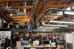
The rise of Neurophos optical processing units highlights a core constraint facing modern AI systems: scaling compute without exploding power use. As AI inferencing expands across data centers, energy efficiency has become the gating factor. Neurophos, an Austin-based photonics startup, is positioning optical hardware as a practical response to this challenge, grounded in material science research that has evolved over two decades.
Spun out of Duke University research and Metacept, Neurophos builds on early metamaterials work that once explored invisibility cloaks. That research later informed advances in electromagnetism. Today, the same scientific lineage underpins a metasurface modulator designed to perform matrix vector multiplication, a foundational operation in AI inferencing workloads.
This shift matters because inferencing, unlike training, must run continuously at scale. As demand grows, efficiency gaps become operational risks rather than theoretical concerns.
Why AI inferencing efficiency has become a power problem
AI inferencing depends on executing trained models repeatedly, often in real time. This workload is currently handled by silicon-based GPUs and TPUs. While effective, these chips generate heat and consume large amounts of power as performance increases.
The Neurophos optical processing units approach reframes this equation. Instead of relying on traditional silicon gates and transistors, the company’s metasurface modulators use optical properties to execute tensor-core-like functions. Light, by nature, produces less heat and is less sensitive to electromagnetic interference.
In theory, photonic chips have long promised these advantages. In practice, size, manufacturing complexity, and conversion overhead between optical and electronic domains have limited adoption. Neurophos claims its approach addresses these constraints at once by shrinking optical transistors dramatically.
Metasurface modulators and the optical tensor core concept
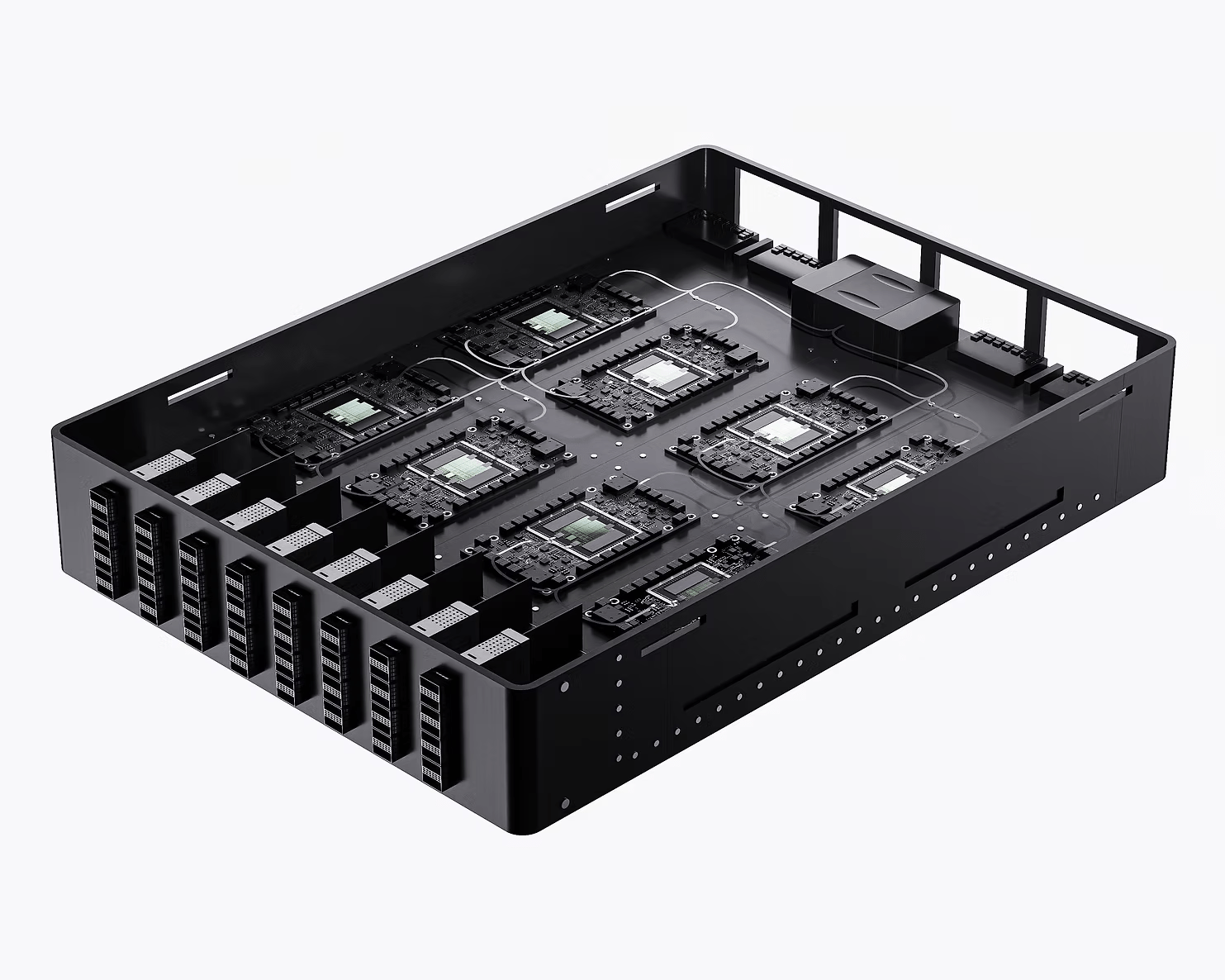
At the center of the Neurophos architecture is the metasurface modulator. According to the company, this component is about 10,000 times smaller than traditional optical transistors. That reduction enables thousands of modulators to fit on a single chip.
The impact is twofold. First, more calculations can occur directly in the optical domain before converting back to electronics. Second, parallelism increases without proportional power growth. The result, the company claims, is an optical processing unit optimized for inferencing rather than general-purpose compute.
This design positions Neurophos optical processing units as purpose-built infrastructure, not experimental hardware. It reflects a broader shift toward specialized accelerators tailored to specific AI workloads.
Performance claims and competitive positioning
Neurophos states that its optical processing unit can operate at 56 GHz, delivering a peak of 235 peta operations per second while consuming 675 watts. The company contrasts this with Nvidia’s B200 AI GPU, which it says delivers 9 peta operations per second at 1,000 watts.
These figures frame the startup’s core claim: performance gains paired with lower energy use. The company argues that solving efficiency first enables speed gains without untenable power costs. This narrative resonates in a market where energy availability increasingly constrains data center expansion.
However, the competitive landscape is crowded. Nvidia dominates AI hardware, and other photonics companies have shifted focus toward interconnects. Neurophos differentiates itself by targeting compute directly and anchoring its roadmap in manufacturing compatibility.
Manufacturing, funding, and the road to 2028
One historical barrier for photonic chips has been mass production. Neurophos counters this by stating its chips can be manufactured using standard silicon foundry materials, tools, and processes. If accurate, this lowers adoption friction and aligns with existing supply chains.
To advance development, the company has raised $110 million in a Series A round led by Gates Frontier, with participation from Microsoft’s M12 and several other venture investors. The funding supports development of an integrated photonic compute system, data center-ready modules, a full software stack, and early-access developer hardware.
The company expects its first chips to reach the market by mid-2028. In the interim, it is expanding engineering operations in San Francisco and Austin, while engaging with early customers.
What this means for AI infrastructure leaders
For CXOs and infrastructure decision-makers, Neurophos optical processing units represent a strategic signal. Incremental gains in silicon efficiency may no longer keep pace with inferencing demand. Optical compute, if manufacturable at scale, introduces a fundamentally different efficiency curve.
This moment mirrors earlier infrastructure inflection points, where physics, not software, set the limits. Leaders evaluating long-term AI roadmaps must weigh whether evolutionary improvements suffice, or whether architectural shifts become inevitable.
In parallel, organizations assessing broader technology strategy can explore enabling services that support such transitions. Explore the services of Uttkrist. Our services are global in nature and highly enabling for businesses of all types. Drop an inquiry in your suitable category: https://uttkrist.com/explore/
As AI hardware diversifies, complementary platforms and solutions will also shape deployment outcomes. Some ecosystems are already forming around next-generation AI tooling and workflows, including emerging platforms such as https://qlango.com/.
How should enterprises balance near-term stability with long-term bets on radically different compute architectures?
Explore Business Solutions from Uttkrist and our Partners’, https://uttkrist.com/explore